the idea
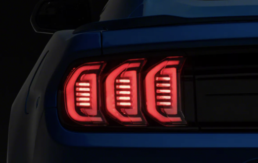
Every modern Mustang has a turn signal that lights its three rear LEDs one at a time, sweeping outward from the center. The animation is a small thing but it's instantly recognizable as a Mustang. As a VLSI exercise it's almost perfect: small enough to fit in one head, big enough to need a proper state machine, with a few corner cases (brake, idle, fault) that turn it into a real design problem instead of a counter.
This was an early homework in ELEC 422 (VLSI System Design) and the warm-up before the bigger Tetris chip. Two architectures, side by side, written in SystemVerilog and pushed through the full standard-cell ASIC flow.
what it does
- Sequential left / right turn signal. Three LEDs per side, lit in sequence, sweeping outward.
- Brake override. When the brake pedal is pressed, both sides switch to solid (non-sequential) so the brake lights are unambiguous.
- Idle state. All LEDs off when nothing's commanded.
- Fault detection. If both turn signals are asserted at the same time (an impossible-in-driving input), the design refuses to animate and flags the fault.
two implementations
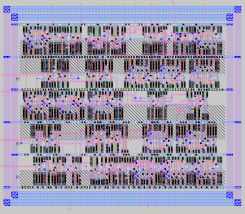
version 1: pure FSM
A single 4-bit state machine encodes every visible state (idle, left-1, left-2, left-3, right-1, right-2, right-3, brake, fault). Each state directly drives the LED outputs combinationally. Easy to reason about, easy to draw on the back of a homework sheet, but state count grows fast if you ever extend it (more LEDs, more behaviors, more fault modes).
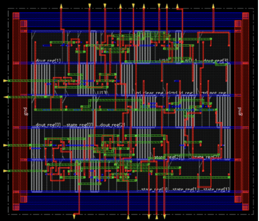
version 2: FSM + Datapath (FSMD)
The same behavior, split between a small controller FSM (idle / sequencing / brake / fault) and a tiny datapath (a counter and a shift register for the LED pattern). The controller issues commands like start_sweep or brake_on; the datapath does the actual bit shuffling. Fewer states, more reusable, and the cleaner pattern to scale up. This is the same FSMD style that the Tetris chip later in the course uses, just with a much smaller datapath.
clocking
Like every design in the class, this one uses two non-overlapping clocks (clka / clkb) generated externally. Next-state logic latches on clka; outputs and datapath registers update on clkb. The phase separation guarantees that by the time the datapath registers fire, every control signal from the FSM has fully settled. Same trick, smaller design.
flow
- RTL in SystemVerilog (with Tcl scripts driving the tools).
- Pre-synthesis simulation in QuestaSim, exercising every transition and the brake / fault corner cases.
- Synthesis with Design Compiler / Genus against the OSU05 standard-cell library.
- Post-synthesis simulation against the gate-level netlist, same testbench, expected to match the pre-synth waveforms exactly.
- Place-and-route in Cadence Innovus, imported to Magic for DRC and padframe.
- Post-layout simulation in IRSIM against the extracted netlist.
why both versions
The point of doing both was to actually feel the tradeoff. The pure FSM is faster to write, the FSMD is cleaner to extend. On a problem this small, both fit in a few hundred lines and synthesize to a handful of cells. The point isn't the chip, it's the muscle memory. Once you've written the same behavior twice in two architectures, the FSMD methodology stops being abstract and starts being the obvious move for anything more complicated.