the pitch
The idea was simple to describe and hard to pull off: a thin, skin-worn patch that captures the same kind of continuous biosignals an Oura ring captures (heart rate, HRV, temperature, motion) but in a form factor that's easier to manufacture at home than a ring is. No injection-molded enclosure, no curved PCB, no specialist assembly. Just a long, thin two-layer board, a coin or small lithium polymer battery, and a piece of medical-grade adhesive on the back.
I prototyped a v1 board, brought it to demo day, and it didn't work. The story of why it didn't work is the actually interesting part.
the board
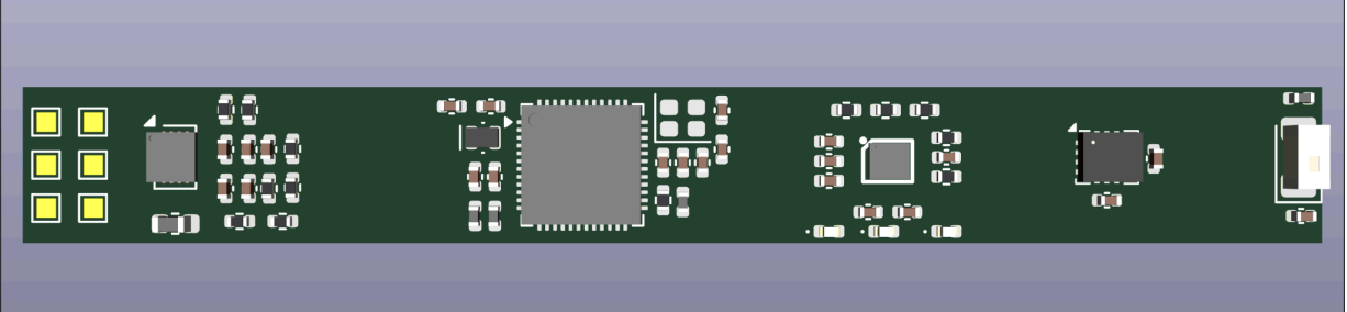
From left to right: an array of optical sensor pads for PPG (the yellow squares), a small sensor frontend IC, the main BLE SoC in the middle with its decoupling network, a secondary IC (motion / IMU), a power-management section, and a USB-C connector at the far right for charging and firmware loading. Everything sits on a board roughly the width of a finger so the patch can flex against the skin without forcing a rigid section onto a soft surface.
schematic
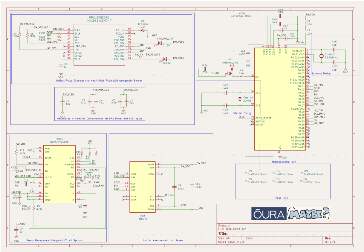
The block-level architecture is what you'd expect for a wearable biosensor: a BLE-capable MCU at the center, a PPG / optical frontend for pulse and oxygenation, an IMU for motion and activity classification, and a charge controller plus regulator for the LiPo battery. The MCU streams sensor data over BLE to a phone, which is where the actual signal processing was meant to live.
what went wrong
The honest answer is that v1 had too many first-time-for-me parts on one board. I'd never laid out a BLE SoC before, never routed a PPG sensor's analog return path before, never integrated a multi-cell charge controller before. Each of those individually is a learnable thing. Stacking all three on the same first-revision board, on a deadline, with no intermediate breakouts to validate each subsystem in isolation, meant that when something on the demo board misbehaved I had no clean way to isolate which subsystem was the culprit.
I went into the demo with a board that wasn't fully bringup-tested, and the demo went exactly how that always goes.
what I'd do differently
- Break it up. v1 should have been three small breakout boards (BLE alone, PPG alone, charge alone) and then a v2 that combines them. The temptation to "just spin one board" is real and I'd push back on it harder next time.
- Bring-up plan written down before fab. A short doc that says "first, verify rail voltages. Then verify MCU enumerates over SWD. Then verify the BLE radio advertises. Then…" The thing that kills demo-day debugging is doing this exploratory rather than methodically.
- Pad out the test points. A few extra labeled test pads cost nothing in board area and save an hour each time you need to scope a signal in a hurry.
- Adhesive matters as much as the silicon. The "patch" only matters if the patch sticks. I underspent attention on the mechanical side of the wearable side of a wearable.
where it went after
A lot of what I learned on Node fed directly into the next hardware project I worked on, which was the NICU monitor with NeoFeed. Multi-layer PCB layout, analog/digital plane separation, debugging mixed-signal designs, all of that started here. The board on this page didn't work. The patterns that came out of building it did.