overview
ELEC 422 was my first introduction to VLSI design. The laborious homeworks of painting transistors on Magic and building finite state machines (FSM's) culminated in a final project that used the datapath-FSM structure to implement a full TetrisASIC. This is how we built it!
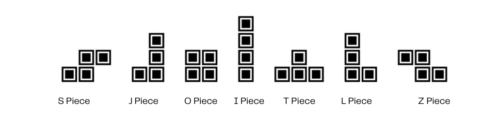
Tetris is played on a 10-column grid where 7 distinct pieces (the S, J, O, I, T, L, and Z tetrominoes) fall from the top. The player moves and rotates each piece before it locks in place. Filling a complete row clears it and scores points. The game ends when pieces stack to the top.
The chip was a final project for ELEC 422: VLSI System Design in Spring 2026, built with my teammates Kathryn Files and Atishay Lalgudi under the team name Memory Mafia. The goal was full functional correctness of every game mechanic (movement, rotation, gravity, line clears, game over) on a fully synthesizable design that could be placed and routed in the AMI 0.5 µm standard-cell flow.
play some tetris first
arrow keys to move · up to rotate · down to drop
credit: tetris engine by straker
architecture
The chip uses the FSM + Datapath (FSMD) methodology taught in the course. It splits into two hierarchical modules: a controller (tetris_fsm) that decides what happens next, and a datapath (tetris_datapath) that does the heavy lifting of moving bits around the board. They sit in a closed loop: status flags from the datapath (collision, full row, game over) feed the FSM's next-state logic, and the FSM in turn issues command pulses and ALU op-codes back to the datapath.
All sequential logic is governed by two non-overlapping clocks, clka and clkb, supplied externally. The FSM latches its next state on negedge clka and drives its outputs on negedge clkb, so by the time the datapath registers fire on clkb, every control signal from the FSM has fully resolved. This phase separation is what makes the design safe to synthesize without race conditions.
controller (tetris_fsm)
A Moore-style FSM that watches the four button inputs (btn_left, btn_right, btn_rotate, btn_drop) and the datapath's status flags. Instead of doing any coordinate math itself, it just issues discrete commands:
- Movement:
alu_op_shift_left,alu_op_shift_right,alu_op_rotate,alu_op_gravity - State management:
piece_lock,piece_spawn,board_reset - Line resolution: triggers the
clear_rowsequence and assertsscore_inc
Main states are IDLE, SPAWN, INPUT_POLL, VALIDATE, UPDATE, LOCK, CLEAR_CHECK, DISP_SCAN, and GAME_OVER. The display scan walks all 20 rows out the bottom each frame with disp_row_valid high.
datapath (tetris_datapath)
This is where the 20×10 board lives. A few constraints from the course flow shaped almost every decision:
No runtime array indexing. Design Compiler in the AMI 0.5 µm flow can't synthesize board[i][j] when i is a variable. So the board is declared as 20 individually named 10-bit registers (board0 through board19), and every read or write happens through a fully unrolled case statement.
Everything combinational is unrolled. Collision detection compares the next piece position against the existing board purely in combinational logic, producing collision_flag in one cycle. Display scanning is a multiplexer tree that fans out the right row onto disp_row_data based on disp_row_addr.
piece mask ROM
All 7 tetrominoes across all 4 rotations are encoded as a combinational lookup table. The key {piece_type, rot_state} indexes 28 entries, each returning a 16-bit mask for the piece's 4×4 bounding box. A separate rot_mask table returns the next rotation, which lets the collision detector pre-check a rotation before the FSM commits to it.
pseudo-random piece selection (LFSR)
A 7-bit LFSR implementing x⁷ + x⁶ + 1 picks the next tetromino. It advances on each falling edge of clkb:
lfsr <= {lfsr[5:0], lfsr[6] ^ lfsr[5]};
That tap configuration gives a maximal-length sequence of 127 states before repeating. To avoid the all-zeros lockup, a free-running 7-bit counter seeds the LFSR at reset (falling back to a hardcoded 7'b1001101 if the counter happens to be zero). The lower 3 bits select the piece type, with 3'd7 remapped to 3'd0 so the distribution stays valid across 7 pieces.
verification
Three rounds of simulation, all driven by the same testbenches:
- Pre-synthesis in Questa. Each module on its own (FSM, datapath, top), verifying spawn, movement, gravity, line clear, and game-over behavior.
- Post-synthesis in Questa. Same testbenches against the gate-level netlist out of Design Compiler. Waveforms matched the pre-synth runs exactly, confirming DC introduced no functional regressions.
- Post-layout in IRSIM. Magic generated a behavioral netlist from the placed-and-routed core, and the same test sequence ran one more time against the core and again through the padframe. Padframe signals are prefixed
p_at the pad boundary and matched the core signals one for one.
synthesis & layout
Synthesized with Design Compiler against the OSU05 standard-cell library (AMI 0.5 µm).
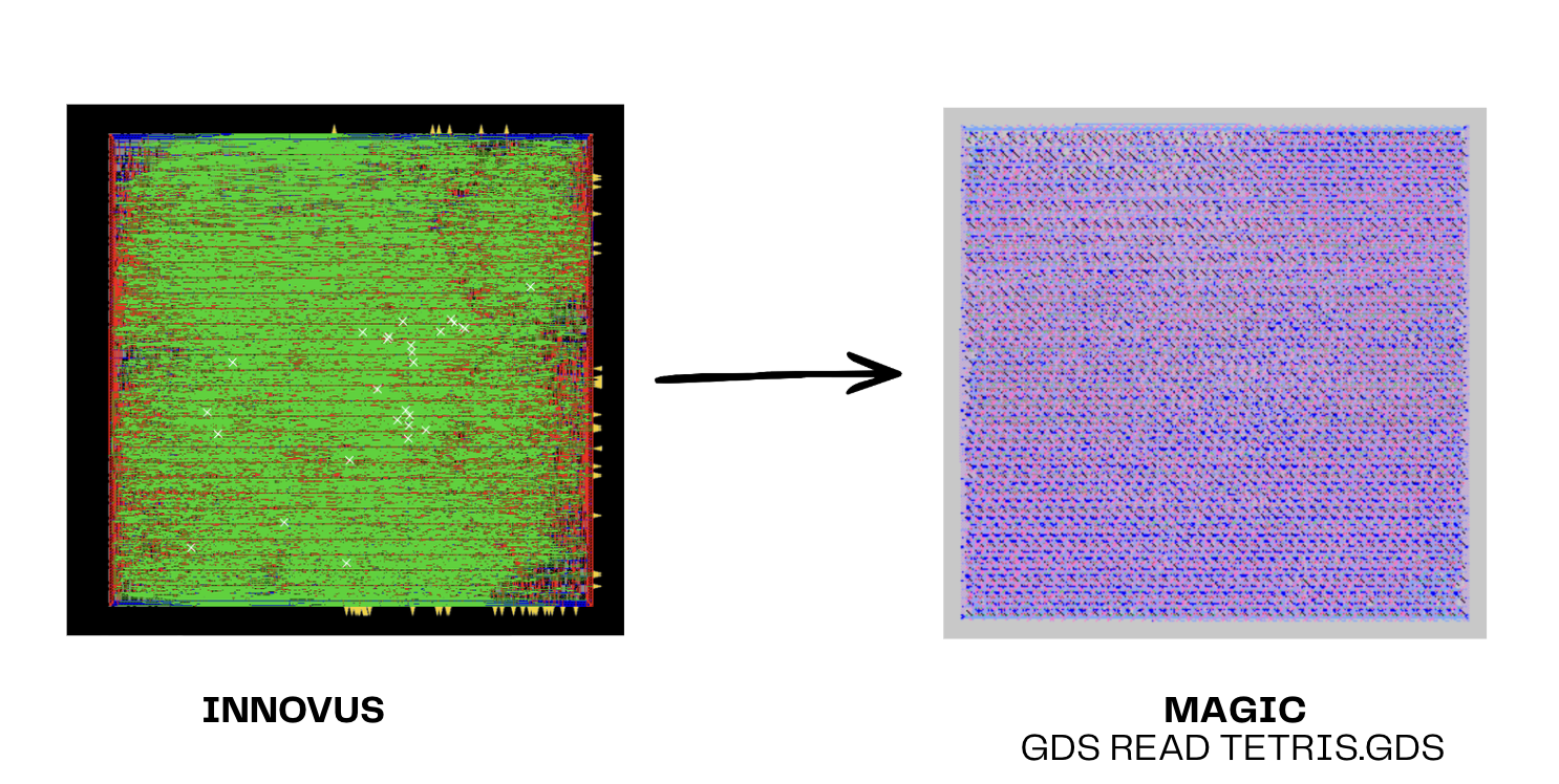
Place-and-route was done in Innovus, then imported to Magic for DRC and padframe integration. The dense, uniform cell arrangement is a direct consequence of the 20 named board registers, the fully unrolled collision detection, and the 28-entry mask ROM.
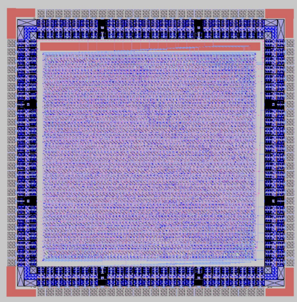
The core needed 61 I/O pins, which overflowed the standard 64-pin padframe once you count VDD/GND, so we used Gavin Jing's padframe generator to build a custom 104-pin padframe. Every signal pin is an OSU bidirectional pad: OEN high drives the pin, OEN low captures it. Unused pads are tied to inputs with OEN low.
testing the fabricated chip
If this design ever came back from fab, the test rig would be:
- 20×10 LED matrix wired to
disp_row_data[9:0]anddisp_row_addr[4:0], gated bydisp_row_valid, with ~100 Ω series resistors per column on 3.3 V - 5 pushbuttons (restart + 4 game inputs) with pull-down resistors
- External dual-phase non-overlapping clock from an FPGA or oscillator, chosen so the 256-cycle gravity tick gives a visible fall rate
- 16 LEDs or a pair of 7-segment displays on
score[15:0], plus single LEDs forout_game_overandout_line_clear
From there it's a stepwise bring-up: assert restart, watch the first piece spawn, exercise each button, let gravity run, stack a full row to confirm out_line_clear and the score increment, then stack to the top to confirm out_game_over.
presentation
Final slide deck from the ELEC 422 tapeout review.
design report
The full design report covers waveform captures from every simulation stage, the FSM state diagram, the Innovus and Magic layouts, the 104-pin pad map, and the bidirectional pad behavior table.